
Markt&Technik | New mass spectroscopy using metrology to combat chip shortages

Originally published in Markt&Technik. (DE)
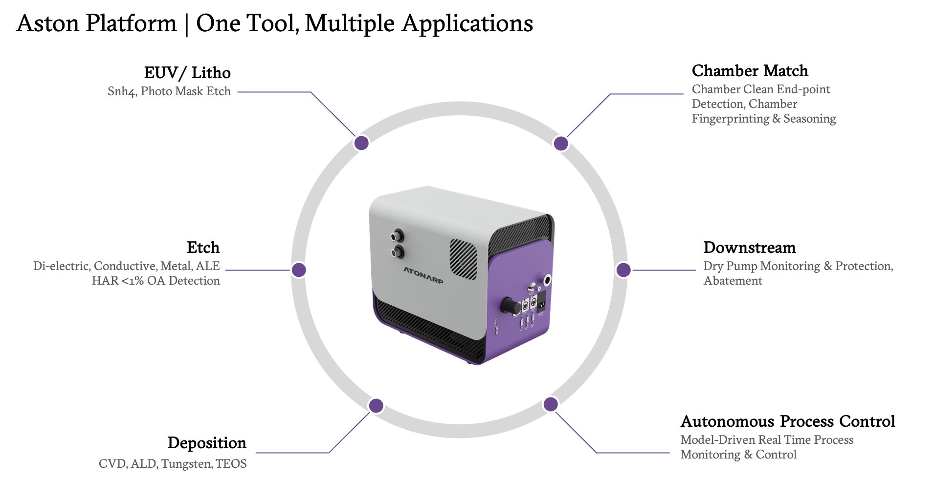
Atonarp aims to significantly increase throughput and yield in IC fabs with its "Aston" mass spectroscopy-based metrology system, newly developed from the ground up for IC manufacturing.
Prakash Murthy, CEO, CTO and founder of Atonarp, is even convinced that with the help of the metrology system called "Aston," a new way of approaching process technology will prevail in fabs. Precisely because "Aston" is able to measure at the molecular level and the data can then be sent to the cloud for analysis.
Overall, equipment and the respective processes could now be better and better aligned, which is known as "Equipment and Process Co-Optimization" (EPCO).
"We're digitizing metrology; we're increasingly getting by without chemicals," Murthy explains.

But what makes "Aston" different from existing metrology systems? First and foremost, corrosive gases generated during many processes cannot harm "Aston."
To understand why this is so important, a quick look at the method that has been used so far. Basically, the Residual Gas Analyzer (RGA) consists of the sensor, the interface box and the control unit. The sensor itself consists of the ion source in which the gas is ionized, the filter and the detector. The ionized molecules are accelerated and deflected by mass and charge in the filter (quadrupole). In the detector it is measured where they arrive and in what quantities. This provides the measurement results.
But this method has a major disadvantage: because in many processes corrosive gases occur as by-products, such as HCI. NF3, which is used for cleaning the process chambers, is also very aggressive. As a result, the ion source electrodes are "eaten up" by the corrosive gases within hours and would then have to be replaced.
Therefore, conventional RGA, which was not originally developed for use in semiconductor process control, is not very suitable: The lifetime of the ion source is very limited and the measurement sensitivity, repeatability and overall accuracy is not very high.
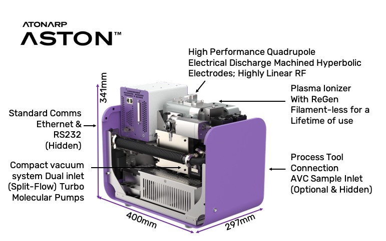
That is why "Aston" has a different design: Here, two different ion sources are integrated, a classical one in which ionization takes place via electrons, and a filament-less plasma ionizer. Corrosive gases can now be introduced into the filament-less ionizer without any problems, because there are no electrodes that could be etched away. The second source with the electrodes is nevertheless important because it is the gold standard for calibrating the filament-less ionizer. Moreover, it can still be used to perform mass spectroscopy in the process steps where no aggressive gases are involved.
In addition, there is another measurement method, Optical Emission Spectroscopy (OES). To perform it, plasma is required in the process chamber. However, if pulsed plasma is used, which occurs in quite a few processes, then OES does not provide reliable results. In atomic layer deposition (ALD) and in atomic layer etch (ALE) processes, such as those being used more and more for the fabrication of 3D NAND flash ICs with many layers and for gate-all-around transistors (GAA), often no plasma is used at all, so OES is out of the question. "So this requires entirely new metrology techniques," says Prakash Murthy. That's what Atonarp was developed, he says, and it generates the plasma itself - so measurements can be made even when no plasma is generated in the actual process.
The end of blind flying
So far, manufacturers have largely been flying blind through the process steps, relying mostly on indirectly collected data and trying to keep to precise timings during the process steps to be reasonably sure that the processes have actually been completed. It would be extremely important to know very precisely when, for example, a certain layer has been completely eliminated by the etching process and the process must be stopped - not before, because unwanted material has not yet been etched away then, and not later, because the following layer is then unintentionally attacked. "End-point detection" is the technical term for this. End-point detection is particularly crucial for the production of 3D NAND memories. This is because very deep holes have to be etched through the many layers with a very high aspect ratio.
The same applies to the cleaning of the process chambers. Here, too, the residues of the reactions are to be removed - but as soon as this is done, the process must be stopped. Otherwise, the cleaning agents will attack the walls of the process chambers, and instead of providing a clean environment for the next wafers, the chambers will then already be contaminated with the substances that were accidentally "cleaned" out of the walls of the chambers - even before the next wafer is introduced. It is therefore important to detect the trace molecules and by-products as well as to accurately detect the end-point of the cleaning process. Over-cleaning is a problem, you can think of it like a good frying pan, for the most consistent results you need your frying pan (and chamber) to be ‘seasoned’ and not over cleaned.

In addition, "Aston" is suitable for characterizing the process chambers. "We can create multi-dimensional profiles of the process over time, resolved by individual molecules, so engineers can understand at the molecular level what exactly is happening. This allows yields to be significantly improved; you can only improve what you measure," Murthy enthuses.
The precise process control even makes it possible to bypass expensive EUV lithography, which is used for the critical process steps because of the shorter wavelength (13.5 nm). The disadvantage of deep UV lithography (248 nm light wavelength) is that the multi-patterning (LELE – litho-etch-litho-etch) required for small process structures entails a lot of etching steps that take time and cost a lot. That's where investing in the more expensive EUV machines pays off. But because "Aston" optimizes the etching processes making them cheaper, deep-UV lithography suddenly offers a more economical alternative again.
The potential of AI is now open
The fact that "Aston" records so much process data "In Situ" is very interesting today for another reason: because the system provides quantitatively determined, chemically specific, usable real-time data on the basis of which AI systems can be trained. "This is exactly the data we can now provide for training, because for the first time we are providing high-quality data at the molecular level, not just pressure and temperature. This now allows the possibilities of AI to be fully exploited," says Martin Mason.


